


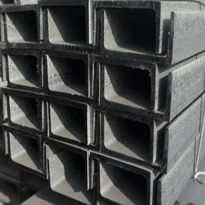


Semiconductor manufacturing demands ultra-precise, corrosion-resistant channels:
Dimensional Precision:
316L stainless steel channels (ASTM A276) with tight tolerances (±0.1mm) maintain 0.5mm clearance for wafer racks, critical for 5nm chip production. Taiwan's TSMC uses U-channels with 80×40×5mm dimensions to prevent particle entrapment.
Chemical Resistance:
Channels with 2.5% molybdenum content resist hydrofluoric acid (HF) exposure, enduring 1,000+ cleaning cycles without pitting. South Korea's Samsung employs these in their 300mm wafer fabs, reducing equipment replacement by 70%.
Surface Finish:
Electro-polished channels (Ra ≤0.02μm) minimize particle adhesion, meeting SEMI F20 Class 1 standards. Japan's Tokyo Electron specifies JIS G4305 SUS316 channels for this critical requirement.
Regional Adoption:
US semiconductor plants use ASTM A479 channels with 6mm minimum thickness, while China's SMIC prefers GB/T 1220 06Cr17Ni12Mo2 channels for cost-sensitive 28nm processes.